الوصف
Introduction
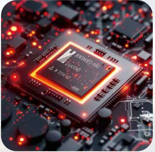
HWD6952-16GLGA52M3 is a high-speed clock driver featuring wide
bandwidth and low jitter performance, with multi-channel time delay
calibration and configurable interface options. This device not only covers
the majority of high-frequency bands (1 GHz to 17 Ghz), but also generates:
Low-frequency clock signals (1 MHz to 1 GHz); Synchronization signals
for multiple pulses; demonstrating strong backward compatibility.
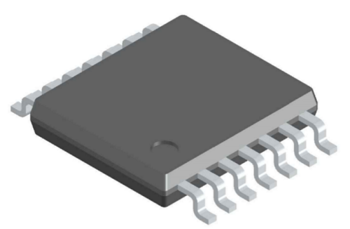
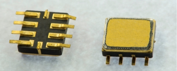
Package: PLGA52; Operating temperature range: -55°C to +125°C.
Main Technical Index
VCO Output Frequency Range: 10-13.5 GHz & 15-17 GHz; Integrated RMS
Jitter: 45 fs (typ.) Integration Range: 100 Hz – 100 MHz; Reference Spur:
< -80 dBc; Normalized Flat Noise Floor: -233 dBc/Hz; Normalized 1/f Noise:
-133 dBc/Hz; External HF Clock Input Range: 8-16 GHz; Number of Output
Channels: 10; Output Delay Adjustment Step: 10 ps (min.); Low Power
Consumption: ≤1.25 W (Total); Single-Supply Operation: 2.5 V.
Application Domains And Scenarios
Wireless infrastructure multicarrier global system for mobile communication
(MC-GSM), 5G; Test equipment and instrumentation; Clock generation;
Aerospace and defense.